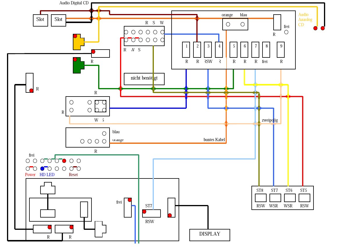
One can now
communicate with the device as symply as echo "hello"> /dev/ttyACM0
or through a terminal like minicum using /dev/ttyACM0 instead of
/dev/ttyS0.
| Instruction |
Code |
Description |
Execution time** |
| RS |
R/W |
DB7 |
DB6 |
DB5 |
DB4 |
DB3 |
DB2 |
DB1 |
DB0 |
| Clear display |
0 |
0 |
0 |
0 |
0 |
0 |
0 |
0 |
0 |
1 |
Clears display and returns cursor to the home position
(address 0). |
1.64mS |
| Cursor home |
0 |
0 |
0 |
0 |
0 |
0 |
0 |
0 |
1 |
* |
Returns
cursor to home position (address 0). Also returns display being shifted
to the original position. DDRAM contents remains unchanged. |
1.64mS |
| Entry mode set |
0 |
0 |
0 |
0 |
0 |
0 |
0 |
1 |
I/D |
S |
Sets cursor move direction (I/D), specifies to shift the
display (S). These operations are performed during data read/write. |
40uS |
| Display On/Off control |
0 |
0 |
0 |
0 |
0 |
0 |
1 |
D |
C |
B |
Sets On/Off of all display (D), cursor On/Off (C) and blink
of cursor position character (B). |
40uS |
| Cursor/display shift |
0 |
0 |
0 |
0 |
0 |
1 |
S/C |
R/L |
* |
* |
Sets cursor-move or display-shift (S/C), shift direction
(R/L). DDRAM contents remains unchanged. |
40uS |
| Function set |
0 |
0 |
0 |
0 |
1 |
DL |
N |
F |
* |
* |
Sets interface data length (DL), number of display line (N)
and character font(F). |
40uS |
| Set CGRAM address |
0 |
0 |
0 |
1 |
CGRAM address |
Sets the CGRAM address. CGRAM data is sent and received after
this setting. |
40uS |
| Set DDRAM address |
0 |
0 |
1 |
DDRAM address |
Sets the DDRAM address. DDRAM data is sent and received after
this setting. |
40uS |
| Read busy-flag and address counter |
0 |
1 |
BF |
CGRAM / DDRAM address |
Reads
Busy-flag (BF) indicating internal operation is being performed and
reads CGRAM or DDRAM address counter contents (depending on previous
instruction). |
0uS |
| Write to CGRAM or DDRAM |
1 |
0 |
write data |
Writes data to CGRAM or DDRAM. |
40uS |
| Read from CGRAM or DDRAM |
1 |
1 |
read data |
Reads data from CGRAM or DDRAM. |
40uS |
Remarks:
- DDRAM = Display Data RAM.
- CGRAM = Character Generator RAM.
- DDRAM address corresponds to cursor position.
- * = Don't care.
- ** = Based on F
osc = 250kHz.
Bit names
| Bit name |
Setting / Status |
| I/D |
0 = Decrement cursor position |
1 = Increment cursor position |
| S |
0 = No display shift |
1 = Display shift |
| D |
0 = Display off |
1 = Display on |
| C |
0 = Cursor off |
1 = Cursor on |
| B |
0 = Cursor blink off |
1 = Cursor blink on |
| S/C |
0 = Move cursor |
1 = Shift display |
| R/L |
0 = Shift left |
1 = Shift right |
| DL |
0 = 4-bit interface |
1 = 8-bit interface |
| N |
0 = 1/8 or 1/11 Duty (1 line) |
1 = 1/16 Duty (2 lines) |
| F |
0 = 5x7 dots |
1 = 5x10 dots |
| BF |
0 = Can accept instruction |
1 = Internal operation in progress |


